

A copper busbar looks like the simplest part in an EV battery pack: a flat strip of metal with a few holes and a bend. In service it carries hundreds of amps, sits next to cells that must not overheat, holds its shape through years of vibration and keeps high voltage where it belongs.
Getting that right is a chain of decisions: alloy and temper, cross-section, bend geometry, plating, insulation and joining method, all within tolerances that let automated lines assemble the pack. This guide walks through each decision the way our engineers review a new copper busbar drawing, with the numbers we use and the mistakes we see most often.
- Use C11000 (ETP) for bolted busbars and C10200 (oxygen free) when the part will be welded or brazed, to avoid hydrogen embrittlement.
- Size the cross-section for temperature rise, not a fixed amps-per-square-millimetre rule; power loss is I²R and depends on cooling.
- Half-hard temper with an inside bend radius of at least one thickness is the usual starting point for formed busbars.
- Tin plating suits bolted joints; nickel suits laser welding to cell tabs; silver suits high current contacts.
- Burrs, sharp edges and damaged insulation cause more high voltage failures than conductivity does.
What a copper busbar does in an EV battery pack
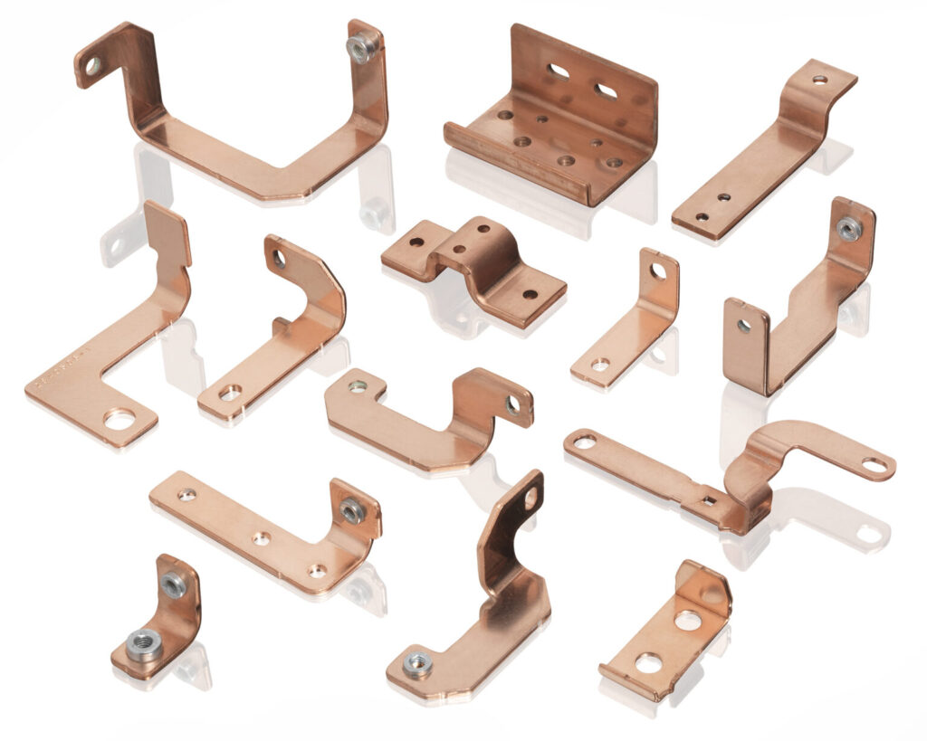
Inside a pack, busbars connect cells into modules, modules into the pack and the pack into the high voltage junction box, contactors, fuses and inverter. Module busbars are usually thin, 0.3 to 2 mm, and welded to cell terminals. Pack and junction box busbars are thicker, 2 to 6 mm, bolted, often bent in three dimensions and insulated along their length. Power electronics add laminated busbars, where several insulated layers sit close together to cut inductance.
Copper wins these jobs because it combines the highest practical conductivity with good strength, easy forming and reliable joints. Aluminum is lighter and cheaper per ampere and is growing in cell-to-cell links, but copper still dominates where space is tight, current is high or the joint must be bolted many times.
Choosing copper busbar material and temper
Most copper busbar drawings call for one of two grades, and the difference matters more than the price suggests.
| Grade | Composition | Conductivity | Use it when | Avoid when |
|---|---|---|---|---|
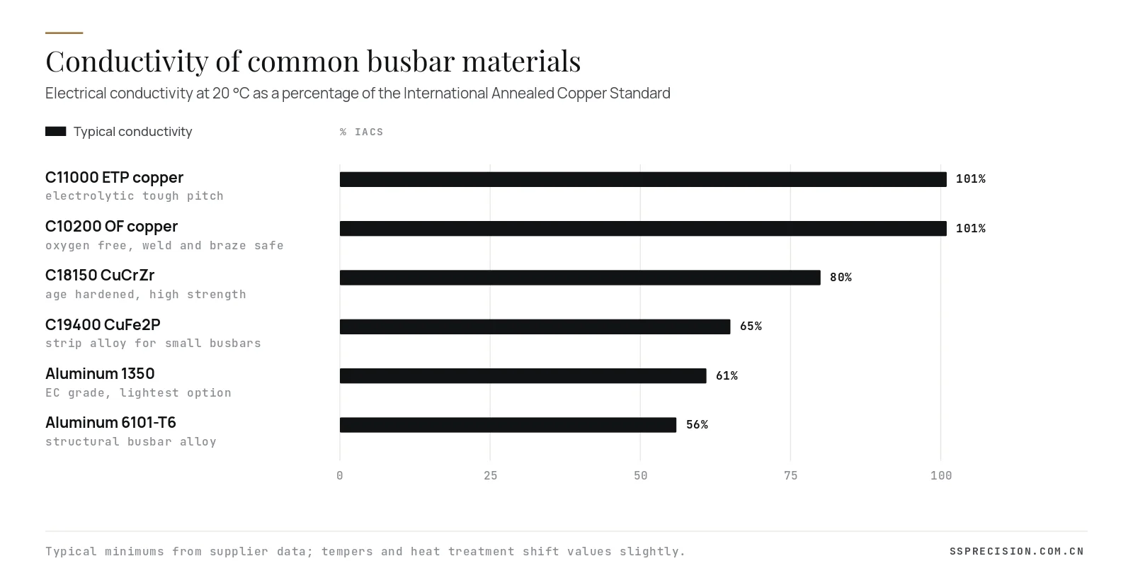
| C11000 ETP | 99.90% Cu, about 0.02 to 0.04% oxygen | 101% IACS min | Busbars are bolted, formed and plated | Parts are brazed or welded in a reducing atmosphere |
| C10200 OF | 99.95% Cu, oxygen free | 101% IACS min | Laser, electron beam or resistance welding, brazing | Budget is tight and no welding is needed |
| C18150 CuCrZr | Cu with about 1% Cr and 0.1% Zr | about 80% IACS | High temperature strength, spring contacts, thin but stiff links | Maximum conductivity is required |
| Al 1350 / 6101 | Aluminum | about 56 to 61% IACS | Weight is critical, joints are welded or specially plated | Joints are bolted without surface treatment |
The reason for oxygen free copper is simple chemistry. ETP copper contains tiny copper oxide particles. When it is heated in hydrogen, as in some brazing or when a weld pool picks up moisture, hydrogen reacts with the oxide to form steam inside the metal, which splits grain boundaries and embrittles the joint. C10200 has no oxide to react, so welded copper busbar designs should specify it.
Temper controls formability. Soft (O60) copper bends tightly but dents and scratches easily. Half-hard (H02) is the usual compromise for pack busbars, holding flatness and hole position while still bending to an inside radius of about one material thickness. Hard tempers need larger radii and show more springback. When a drawing shows sharp bends in thick bar, we often recommend a softer temper or a relief groove rather than risk cracking on the outside of the bend.
Sizing a copper busbar for current and temperature
Rules of thumb such as a fixed number of amps per square millimetre are a starting point, not a design. What matters is how hot the copper busbar gets, which depends on current, resistance and how well heat escapes to air, coolant or the structure.
A worked example: a 40 × 3 mm copper busbar (120 mm²), 300 mm long, carrying 300 A continuous. Resistance is 1.724 × 10⁻⁸ × 0.3 / 120 × 10⁻⁶, about 43 µΩ, so it dissipates about 3.9 W at 20 °C. At an operating temperature of 80 °C, resistance rises about 23% and loss approaches 4.8 W. Whether that is acceptable depends on the thermal path; in a sealed pack with little airflow it may push the bar well above the cell temperature limit, so the cross-section or cooling contact must grow.
Joints matter as much as the bar. A bolted joint with a poor surface can add more resistance than the whole busbar. Design contact faces large and flat, specify plating on the contact area, and use the torque and washer stack the joint was tested with.
Skin effect in inverter and converter busbars
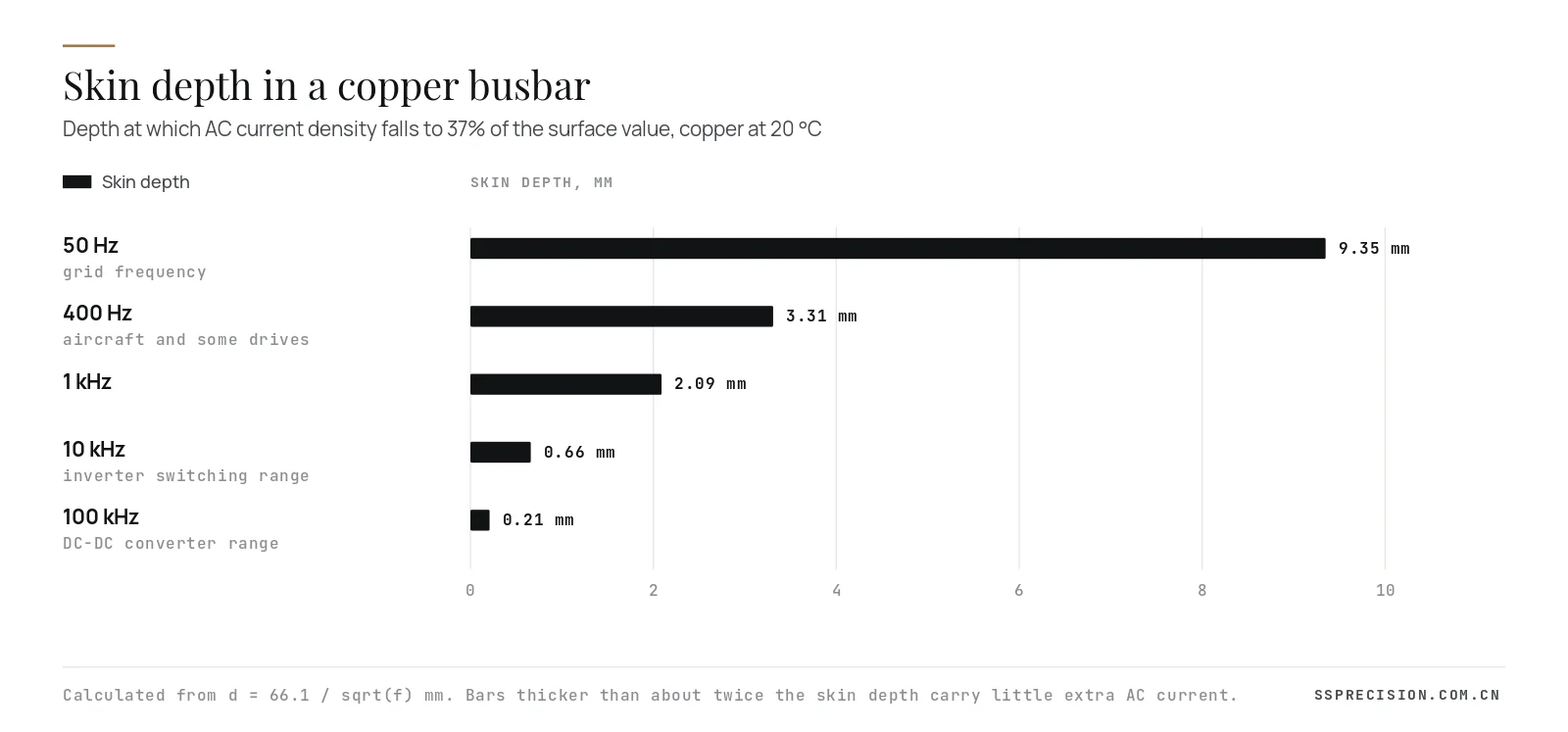
For DC and low frequency current the whole section conducts. At switching frequencies, current crowds toward the surface. The skin depth in copper falls from about 9 mm at 50 Hz to well under 1 mm at 10 kHz, so a thick copper busbar carrying switching ripple wastes material in its core. Wide, thin and laminated busbars are the answer in inverters, which is also why they have lower inductance.
Stamping and bending a copper busbar
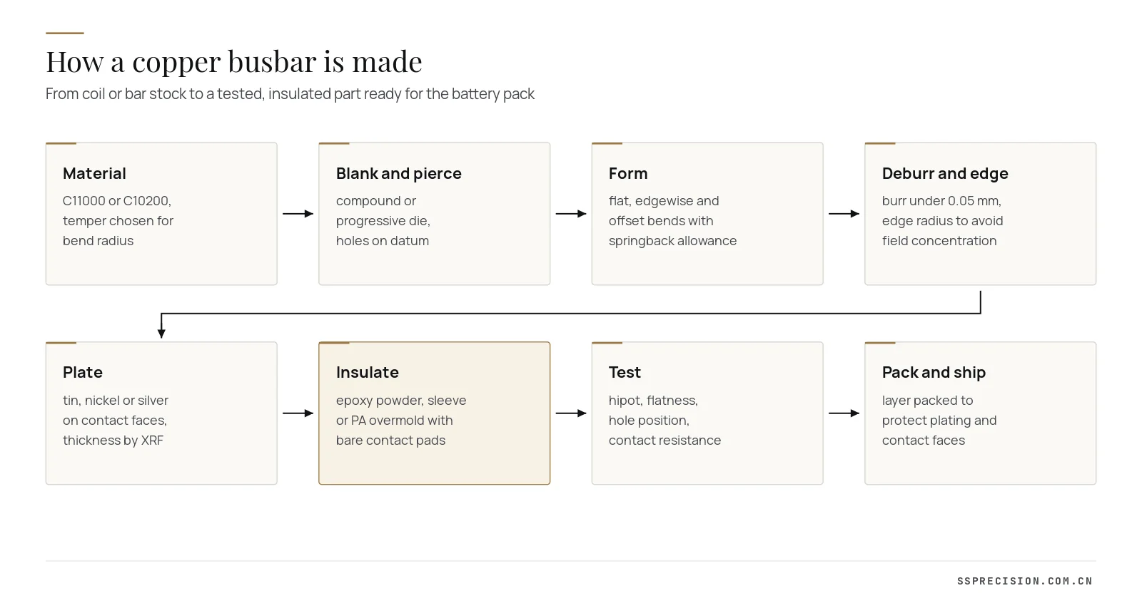
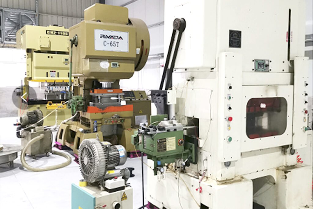
Prototype busbars are often laser cut and formed on a press brake. That is fine for ten parts and costly for ten thousand. In production, we blank and pierce in a compound or progressive die and form in dedicated bending dies, so every hole and bend is located from the same datums and the process stays repeatable at high volume.
Copper is soft and sticky, which shapes the tooling:
- Punch to die clearance: about 5 to 8% of thickness per side for half-hard copper gives a clean shear band and a small burr. Too little clearance galls; too much leaves a heavy burr.
- Burr control: we aim for burrs under 0.05 mm and orient any remaining burr away from insulation and contact faces. On high voltage parts, edges are tumbled or coined to a radius.
- Springback: copper springs back less than steel, but three-dimensional busbars with several bends stack up errors. Bend dies are compensated from first-article measurements, and critical bends are coined or set.
- Edgewise bends: bending a bar across its width needs special tooling to stop the inner edge buckling and the outer edge thinning.
- Surface protection: copper marks easily, and scratches on contact faces raise joint resistance, so dies are polished and parts are handled on protective carriers.
Typical production tolerances for a stamped copper busbar are ±0.1 mm on hole positions relative to datums, ±0.5° on bend angles, and flatness of about 0.1 mm per 100 mm on contact faces. Tighter values are possible with coining and fixtures, but they should be reserved for the features the assembly line actually locates on.
Plating options for a copper busbar
Bare copper oxidizes and its contact resistance drifts. Plating stabilizes the surface and suits it to the joining method.
| Finish | Typical thickness | Best for | Notes |
|---|---|---|---|
| Tin, matte or bright | 3 to 8 µm | Bolted joints, general pack busbars | Low cost, soft contact surface; limit temperature to about 105 to 125 °C |
| Nickel | 3 to 5 µm | Laser welding to cell tabs, higher temperatures | Hard, stable, good weld coupling; slightly higher contact resistance |
| Silver | 3 to 5 µm | High current contacts, contactors, junction boxes | Lowest contact resistance; tarnishes, costs more |
| Selective plating | as above | Plating only contact pads | Saves cost where insulation covers the rest |
Thickness is measured by X-ray fluorescence on contact areas, not averaged across the part.
Insulating a high voltage copper busbar
In 400 V and 800 V packs, every copper busbar outside a sealed module needs insulation except at its contact pads. The common options are epoxy powder coating, typically 0.3 to 1.0 mm thick; heat shrink or extruded sleeves in polyolefin or PET; and injection overmolding in PA or PPS for complex shapes that also need mounting features. Overmolding adds cost to the tooling but gives consistent wall thickness and can integrate clips and bosses.
Whatever the method, insulation fails at edges and corners first. That is why deburring and edge radius are part of the insulation specification, not just the stamping one. Each part is hipot tested, commonly in the range of 2.5 to 4 kV DC depending on pack voltage and the customer standard, and insulation thickness is checked at edges as well as flat faces.
Joining: bolted, welded and ultrasonic busbars
Bolted joints are serviceable and tolerant of mixed materials, but they need controlled torque, flat plated faces and often conical spring washers to keep pressure as the joint heats and cools. Laser welding dominates cell-to-busbar links because it is fast, local and automated; it needs clean surfaces, nickel or bare copper at the weld zone and tight gap control, which again comes back to flatness from the stamping die. Ultrasonic welding joins thin copper and aluminum layers without melting, useful for foil stacks and bimetal links.
Copper to aluminum joints deserve special care. The two metals form brittle intermetallic compounds when fused, and in the presence of moisture they corrode galvanically. Practical solutions include friction or ultrasonic welded bimetal transition pieces, nickel or tin plating on the copper side of bolted joints, and sealing the joint from humidity. If your design mixes an aluminum module link with a copper busbar at the pack level, define the transition method early, because it changes the plating and tooling of both parts.
Laminated copper busbar designs for power electronics
Inverters and DC-DC converters switch hundreds of amps in nanoseconds, and any loop inductance in the DC link produces voltage overshoot across the semiconductors. A laminated copper busbar solves this by stacking the positive and negative conductors as thin, wide plates separated by a film insulator such as PET, PEN or polyimide, 0.1 to 0.5 mm thick, and bonding the stack under heat and pressure. Because the opposing currents flow a fraction of a millimetre apart, their magnetic fields cancel and stray inductance falls to a few nanohenries.
From a manufacturing point of view, each layer is still a stamped copper busbar, but flatness, burr height and hole alignment between layers become far more critical. A 0.05 mm burr can pierce a 0.125 mm film during lamination. We therefore coin edges on laminated layers, pierce all layers from common datums and check creepage distances around every terminal after lamination.
Inspection plan for a production copper busbar
A good control plan measures what the assembly line and the electrical design depend on, and nothing more. The table shows the checks we typically run on each copper busbar part number.
| Characteristic | Method | Frequency |
|---|---|---|
| Hole position and size | Checking fixture or vision system; CMM at first article | Every lot, first and last parts |
| Bend angles and 3D profile | Dedicated gauge; CMM or scan at first article | Every lot |
| Flatness of contact faces | Surface plate and feeler gauge or height gauge | Every lot |
| Burr height and edge condition | Profile projector or optical microscope | Every lot, after each die sharpening |
| Plating thickness | X-ray fluorescence on contact pads | Every plating batch |
| Plating adhesion | Bend or tape test | Every plating batch |
| Insulation thickness and dielectric strength | Thickness gauge; hipot test | Thickness sampled, hipot on every part |
| Material certificate and conductivity | Mill certificate; eddy current conductivity check | Every coil or bar lot |
What drives copper busbar cost
Copper itself is usually the largest share of the price, so material utilization matters. A copper busbar nested badly in the strip or bar can waste 30% or more of the metal, while a well designed strip layout, or a small change in part shape agreed at design review, can recover much of that. Scrap copper has resale value, but less than its purchase price.
After material, the main cost drivers are the number of bends and their complexity, plating area and type, insulation method, and inspection. Silver plating and overmolding add the most. Tooling is a one-time cost that falls quickly per part as volume rises; for most pack programs above a few thousand sets per year, hard tooling beats laser cutting and press brake forming on both price and consistency.
Common copper busbar defects
- Cracks on the outside of bends: radius too tight for the temper, or a bend line running along the rolling direction.
- Hole position drift after bending: holes pierced after forming, or located from a bent edge rather than a datum.
- Plating blisters: poor cleaning before plating, or oxide left from annealing.
- Hipot failures at edges: burrs or thin insulation on sharp corners.
- Hot joints in service: uneven contact faces, damaged plating or incorrect bolt torque.
Eight best practices for a copper busbar program
- Specify C10200 whenever the part is welded or brazed.
- Size the section from a thermal model or test, including joint resistance.
- Pierce holes before bending and dimension them from the same datums the assembly uses.
- Use half-hard temper and an inside radius of at least one thickness unless testing proves otherwise.
- Set a burr limit and an edge radius on the drawing for every high voltage part.
- Choose plating by joining method: tin for bolts, nickel for laser welds, silver for high current contacts.
- Keep insulation off contact pads with masking or overmold shut-offs, and hipot test every part.
- Plan tooling for volume: laser and press brake for prototypes, dies for production.
Moving a copper busbar from prototype to production?Send the 3D model and annual volume. We will propose the blanking and forming tools, plating route and inspection plan with a quote.
Request a quoteCopper busbar tooling and parts from SSP
We design and build the dies behind busbar programs and run parts for customers who prefer to buy finished busbars. Blanking and piercing run on compound and progressive dies; formed busbars and deep drawn battery covers run on transfer dies; and overmolded busbars use our insert molding tooling. Every part family gets a control plan covering hole position, bend angle, flatness, burr height, plating thickness and hipot.
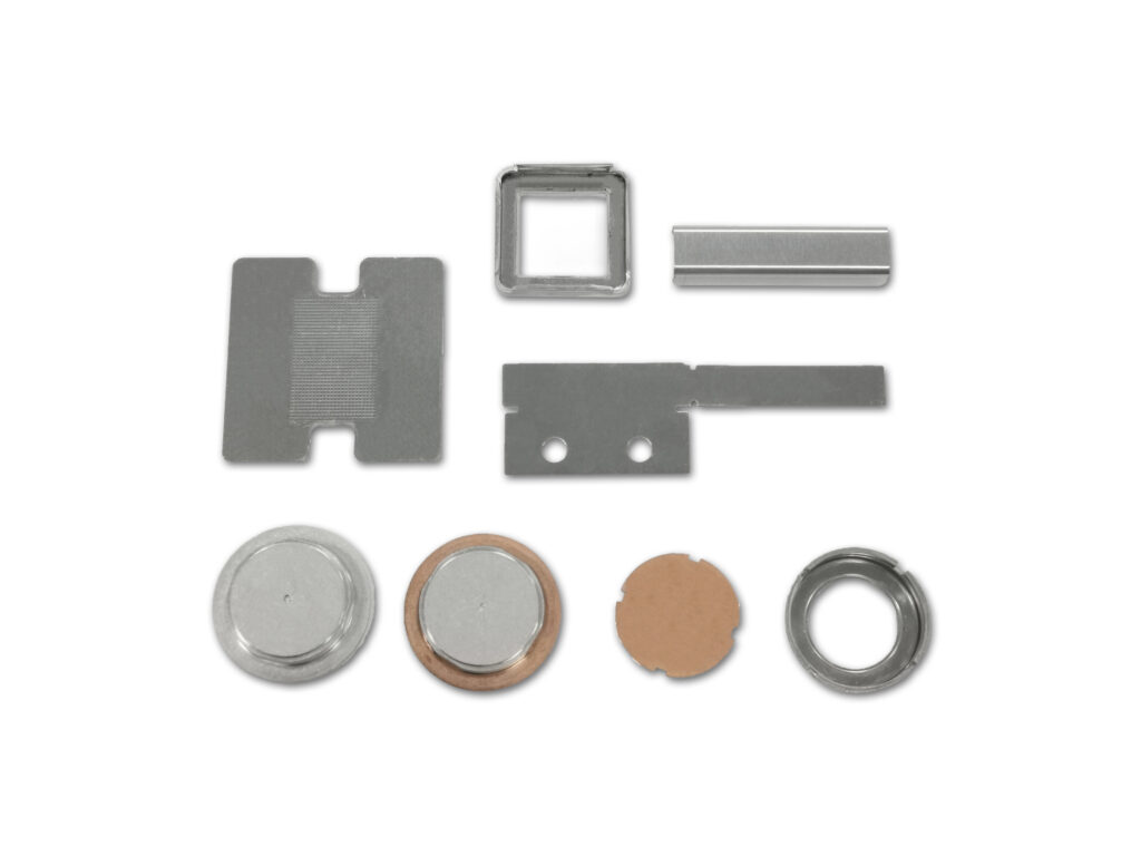
For more on the tooling side, see stamping die manufacturing and our guide to what drives metal stamping die costs. Material data for copper alloys is published by the Copper Development Association.
Copper busbar FAQ
What copper grade is best for EV busbars?
C11000 ETP copper is the standard for bolted busbars. C10200 oxygen free copper should be used when busbars are laser welded, resistance welded or brazed, because it cannot suffer hydrogen embrittlement.
How much current can a copper busbar carry?
It depends on the allowed temperature rise and cooling, not only on cross-section. Calculate resistance with R = ρL/A, find the loss with I²R, and confirm temperature by thermal modelling or test at the real mounting conditions.
Should a copper busbar be tin or nickel plated?
Tin plating of 3 to 8 µm suits bolted joints at moderate temperature. Nickel of 3 to 5 µm suits laser welding and higher temperatures. Silver is used for the lowest contact resistance at high current.
What is the minimum bend radius for a copper busbar?
For half-hard copper, an inside radius of about one material thickness is a safe starting point. Soft copper can bend tighter; hard tempers and thick edgewise bends need larger radii or special tooling.
How are copper busbars insulated?
Common methods are epoxy powder coating, heat shrink or extruded sleeves, and injection overmolding. Contact pads are masked or shut off, and every part is hipot tested to the pack’s voltage specification.