Precision microelectronics injection molding service for global tech OEMs. Learn how micro injection molding delivers tight-tolerance electronic components with IATF 16949 certified quality.
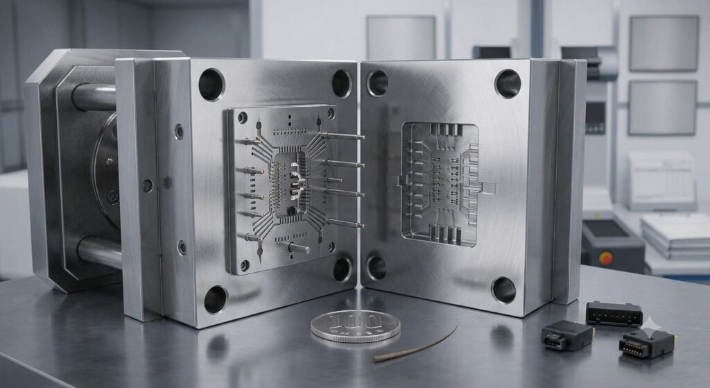
Microelectronics components continue to shrink in size while demanding ever-tighter tolerances and higher production volumes. Microelectronics injection molding has emerged as the preferred process for producing precision plastic parts used in consumer electronics, wearable devices, automotive electronics, medical sensors, and IoT modules. Unlike conventional molding, micro molding requires specialized tooling with micron-level precision, advanced material science, and stringent process control. This article explores how precision injection mold makers deliver reliable, high-volume micro-molded components that meet the rigorous quality and delivery demands of global tech OEMs across multiple industries.
Key Takeaways
- Micro injection molding achieves tolerances as tight as ±0.01 mm on parts weighing less than a gram.
- It demands specialized mold steels, precision EDM and CNC machining, and certified quality systems such as IATF 16949 and ISO 9001:2015.
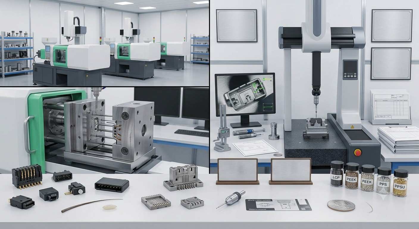
- In-house metrology with CMM and vision systems validates every critical dimension before shipment.
Micro Molding at a Glance
| Parameter | Typical Information |
| Typical tolerance | ±0.01 – 0.03 mm |
| Part weight range | 0.01 – 10 g |
| Common materials | LCP, PEEK, PA66, PPS, PC/ABS, LSR |
| Certifications | ISO 9001:2015 / IATF 16949 |
| Typical annual volume | 100K – 50M parts/year |
| Industries served | Consumer electronics, automotive, medical, IoT |
What Is Microelectronics Injection Molding?
Microelectronics injection molding is the process of forming miniature plastic components using precision-engineered mold cavities measured in microns. These molds feature microscopic gate systems, ultra-thin wall sections (down to 0.1 mm), and precision ejector pins that handle delicate parts without deformation.
The process differs fundamentally from conventional molding. Injection pressures are higher, cycle times are optimized for small shot volumes, and mold temperature control must be precise to prevent premature solidification in micro channels. Every element is engineered for repeatability across millions of cycles.
Why Micro Molding Matters for Electronics OEMs
Global electronics OEMs face constant pressure to miniaturize without sacrificing reliability. Connectors, sockets, sensor housings, and lens arrays must fit into ever-shrinking device envelopes while maintaining mechanical strength, electrical insulation, and thermal resistance.
Micro injection molding solves this by producing net-shape components with consistent quality at high volumes. For OEMs sourcing from Asia, working with a certified mold maker like SSPrecision means access to mature supply chains, competitive tooling costs, and ISO-compliant quality systems that satisfy global procurement requirements.
Common Microelectronic Parts and Their Requirements
The table below summarizes typical micro-molded parts found in electronic devices, the materials specified, achievable tolerances, and common applications. This reference helps engineers and buyers align part design with manufacturing capability.
| Part Type | Typical Material | Tolerance (mm) | Mold Steel | Application |
| Board-to-board connectors | LCP | ±0.01 | S136 / 1.2083 | Smartphone, tablet internal connections |
| BGA / IC sockets | PPS / PEEK | ±0.01 | 1.2343 ESR | Processor and test sockets |
| Sensor housings | PA66 / PBT | ±0.02 | 1.2343 / H13 | Automotive and industrial sensors |
| Micro switches | LCP / PA9T | ±0.01 | Stavax / 1.2316 | Consumer electronics, appliances |
| LED lens arrays | PC | ±0.02 | 1.2738 | Lighting, display backlighting |
| Wafer / carrier trays | PEEK / PES | ±0.03 | 1.2316 | Semiconductor handling |
| Miniature enclosures | PC/ABS | ±0.02 | 1.2738 | Wearables, IoT modules |
Each part type presents unique challenges. Connectors demand flatness and dimensional stability across thousands of cavities. Lens arrays require optical-grade surface finish with zero flow marks. SSPrecision selects the appropriate mold steel and machining strategy for each application to ensure tool longevity and part consistency.
Materials Used in Micro Injection Molding
Material selection is critical in microelectronics. LCP (Liquid Crystal Polymer) offers high-temperature resistance and dimensional stability for connectors and switches. PEEK provides chemical resistance and mechanical strength for sockets and semiconductor components.
PA66 (Nylon) and PBT serve sensor housings and structural parts that require good impact strength. PC/ABS blends are common for enclosures needing a balance of toughness and cosmetic finish. For applications requiring flexibility and temperature resistance, liquid silicone rubber (LSR) is used for micro seals and gaskets.
Required Tolerances and Quality Standards
Microelectronic components routinely require tolerances of ±0.01 mm or tighter on critical dimensions such as pitch spacing, cavity depth, and wall thickness. Achieving this consistently across millions of parts demands robust process capability (Cp/Cpk ≥ 1.33) and rigorous inspection protocols.
SSPrecision maintains an in-house CMM and metrology lab equipped with vision measurement systems, surface roughness testers, and hardness testers. First-article inspection reports (FAIR) and process capability studies are provided for each production run, giving OEMs full traceability and quality documentation.
IATF 16949 and ISO 9001: Why Certification Matters
Global tech OEMs require their mold suppliers to hold recognized quality certifications. ISO 9001:2015 demonstrates a commitment to consistent quality management, while IATF 16949 adds automotive-grade requirements for risk management, defect prevention, and continuous improvement.
These certifications are not just paperwork. They mandate documented procedures for mold design review, material traceability, calibration of inspection equipment, and corrective action when deviations occur. For an OEM evaluating a new supplier, certification is often a non-negotiable gate criterion.
The SSP Micro Molding Workflow: From Design to Delivery
SSPrecision follows a structured process starting with design for manufacturing (DFM) review, where each cavity layout, gate location, and ejection strategy is optimized before steel is cut. Mold design is followed by steel selection based on part material and volume requirements.
Precision machining combines high-speed CNC milling and EDM (wire and sinker) to achieve cavity geometry within tolerance. After assembly and tryout, first-shot samples are measured in the metrology lab. Once approved, production proceeds with in-process sampling at defined intervals. SSP has delivered tooling to 30+ countries since 2008, serving automotive, electronics, and medical customers.
Cost and Lead-Time Considerations for Micro Molds
Micro molds typically cost more than conventional molds due to tighter tolerances, finer surface finishes, and the use of higher-grade mold steels such as Stavax, S136, and 1.2343 ESR. Lead times range from 4 to 10 weeks depending on cavity count, complexity, and material selection.
The total cost of ownership, however, often favors precision micro molds. A well-built mold from an experienced maker delivers longer tool life, fewer rejected parts, and less downtime — directly improving the OEM’s cost per part at high volumes.
SSP Is a Trusted Partner for Die Manufacturing Cost Optimization
SSP Precision is an ISO 9001 & IATF 16949 certified manufacturer delivering end-to-end precision solutions—from DFM engineering and rapid prototyping to high-volume production—for the automotive, medical, electronics, aerospace, and industrial sectors. We handle every stage in-house to manufacture the tooling that makes your parts and the parts themselves.
Visit our to explore our full capabilities: ssprecision.com.cn
Services (tooling design & manufacturing)
- Stamping Dies Manufacturing – high-volume metal stamping with Progressive Die Stamping & Tooling spare parts manufacturing and Transfer Stamping Dies
- Injection Molding – custom plastic molds including Over Molding & Insert Molding and Liquid Silicone Rubber (LSR) Molding
- Green Mold – eco-friendly molded components, Micro Molding – microscopic medical precision parts
Products (end-use parts & spare components)
- Stamping Die – complete stamping tooling
- Injection Mold – complete injection tooling
- Tooling Spare Parts – punches, inserts, ejector pins, Robotics Spare Parts – precision automation spares , Ball Screw Repair Kits – replacement kits for motion systems
- Machine Parts – general precision machine components
Frequently Asked Questions
What is the typical tolerance for micro injection molding?
- Typical tolerances range from ±0.01 mm to ±0.03 mm, depending on part geometry, material, and cavity design.
What materials are most commonly used in microelectronics molding?
- LCP, PEEK, PA66, PPS, and PC/ABS are the most common, with material choice driven by thermal, mechanical, and electrical requirements.
How long does it take to manufacture a micro injection mold?
- Typical lead times range from 4 to 10 weeks, influenced by cavity count, geometry complexity, and mold steel availability.
What certifications should a micro mold supplier hold?
- ISO 9001:2015 is the baseline. For automotive or high-reliability electronics, IATF 16949 certification is strongly recommended.
Can micro injection molding achieve optical-grade surface finish?
- Yes. With polished mold cavities and controlled processing parameters, optical-grade surfaces are achievable, particularly in PC and PMMA lens applications.
How does micro molding compare to metal stamping for electronic parts?
- Micro molding offers greater design freedom, lower tooling cost for complex geometries, and the ability to integrate multiple features into a single part. Stamping remains preferred for high-volume metallic contacts and shields.
Microelectronics injection molding enables global tech OEMs to produce increasingly miniaturized components without compromising on precision, reliability, or production scalability. The process demands specialized tooling expertise, certified quality systems, and rigorous metrology.
Contact SSPrecision to discuss your next micro molding project or request a DFM review. With ISO 9001:2015 and IATF 16949 certification, in-house CMM metrology, and over 15 years of precision tooling experience, SSP delivers micro molds that perform at production scale.
Read More – Intelligence That Protects Your Production Line
- Average Lead Times for China Tooling Production – Stamping dies take 4–12 weeks and injection molds 3–14 weeks depending on complexity, steel grade, and tolerance requirements.
- Should You Source Molds in China or Locally? – China molds cost 40–60% less with 3–6 week lead times, while local sourcing offers tighter tolerances and faster design iterations.
- How to Prevent Flash, Warpage & Sink Marks – Flash, warpage, and sink marks account for 35–40% of plastic part rejects—here’s how to eliminate them with precision tooling and process control.
- Complete Plastic Shrinkage Chart (ABS, PC, PA66, POM) – ABS shrinks 0.4–0.7%, PC 0.5–0.7%, PA66 1.0–2.0%, and POM 0.6–1.4%—here’s how to adjust your mold design for each material.
- Export-Ready Tooling & Dies: OEM Manufacturing for Global Supply Chains – IATF 16949-certified stamping dies, injection molds, and tooling spare parts under one roof for automotive and industrial OEM buyers.
- Multi-Cavity Injection Molds: Cost & Efficiency Breakdown – A 4-cavity hot runner mold costs 2.5–4x a single-cavity tool but delivers proportionally larger per-part cost savings at volume.
- Sourcing Ejector Pins & Mold Components in China – DIN 1530 ejector pins at $5.80–$8.60 per piece with ±0.002mm grinding precision and 7–15 day lead times.
- China Fiber Optic Connectors | Injection Molding Precision Parts Manufacturer Company – Fiber optic connector housings demand ±0.01 mm tolerances on critical alignment features.
- Reducing Cycle Time Through Better Mold Cooling – Cooling eats 50–70% of your cycle time—conformal channels can slash it by 20–50%.
-
Stamping Dies Manufacturing: Custom Dies for OEMs – Custom stamping dies achieve ±0.002 mm tolerances for high-volume production of automotive, electronics, and medical components.
-
China Injection Mold Source: High-Cycle Multi-Cavity Production Plastic Molds – Multi-cavity molds produce 4–32+ parts per cycle with tolerances to ±0.002mm—here’s how to source high-volume tooling from China.
-
Heavy Duty Transfer Tooling: Multi-Station Transfer Dies for Deep-Drawn Components – Transfer dies handle individual blanks for deep-drawn and heavy gauge parts up to 8mm thick with tolerances to ±0.002mm.
- LSR Injection Molding | Precision Liquid Silicone Rubber – LSR injection molding cures at 5 seconds per millimeter of wall thickness with tolerances to ±0.002mm